I recently decided to do some keyboard hacking for fun, so I started with one of the cheapest Logitech wireless keyboard models available: the K360. This model is a little old and the main chip inside it, as well as the Logitech Unifying wireless protocol it uses, have been well covered before. See Marc Newlin’s MouseJack presentation, Travis Goodspeed’s nRF24 sniffing work, and the KeyKeriki research mentioned in each. I’m doing this more as an exercise rather than novel research, and I didn’t know what I’d find going in. That said, I thought this was a neat little example of extracting bare metal firmware from on-chip flash.
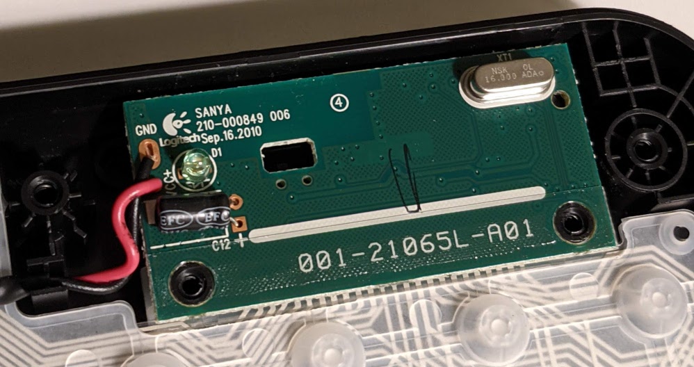
I’m taking a hardware-first approach to reverse engineering the keyboard, so the first step is to extract the firwmare. Disassembling the keyboard is pretty easy after removing the adhesive plate from the front, which exposes all the screws keeping the shell together. Inside there’s the rubber dome key matrix and a small PCB with very few components on it. It’s basically just an nRF24LE1 chip:
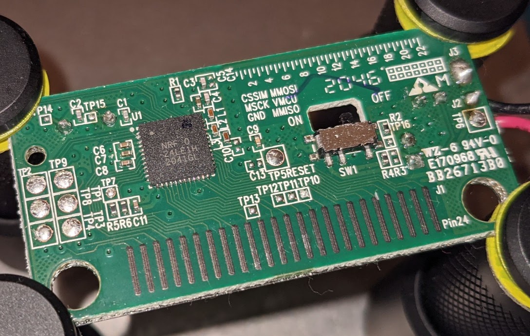
On the left of the nRF24LE1 there’s a grid of six large test pads. This seemed like an interesting interface to poke at, so I checked these pads first using a logic analyzer and some pogo pin probes. TP8 seemed to pulse out a short clock at boot, and TP4 was ground, but I didn’t observe much interesting activity here with passive probing. It became clear that the group of six words silkscreened on the upper right of the board were labels for these test pads due to the clock, ground, and VMCU label positions all matching up with the corresponding pad positions.
To actively probe the SPI interface I then wired up the test pads to a header using some enameled wire. I also wired up TP5 and TP7. According to the nRF24LE1 datasheet, TP7 connects to the PROG pin which is used to “enable flash programming,” and TP5 connects to RESET (also labelled right next to TP5). Reset is active low in this case.
I left the smaller test pads 10-13 alone at this point because they connected to generic GPIO pins and sat on the traces out to the key matrix.
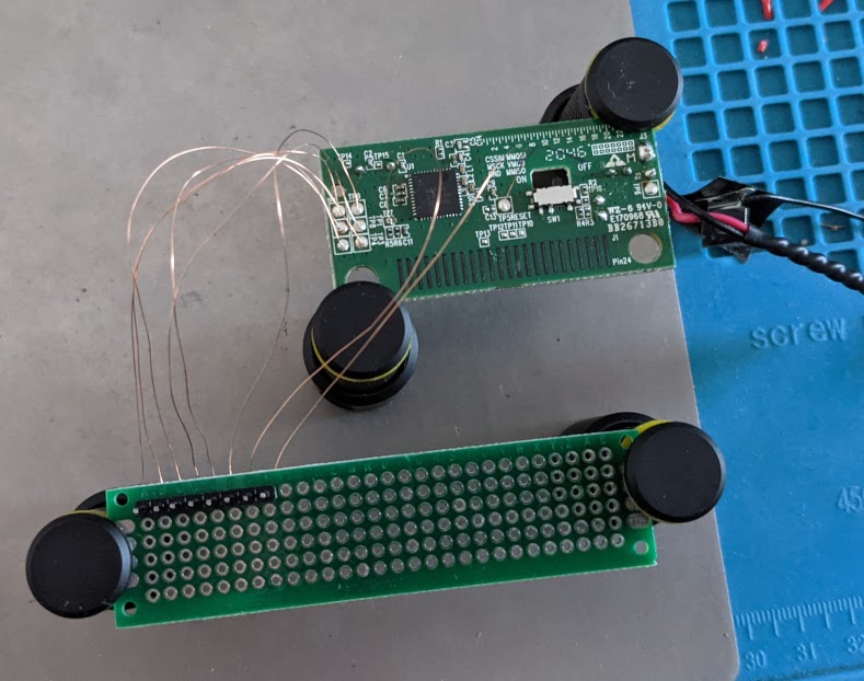
I connected the SPI pads to the default SPI pins on the GreatFET, GND to one of the ground pins, and assigned a GPIO pin for the reset pad. I also used a 3V3 pin on the GreatFET to directly power the nRF24 chip through the VMCU pad.
gf = GreatFET()
reset_pin = gf.gpio.get_pin('J1_P4')
reset_pin.high()
I tried to send some simple test commands using the built-in SPI code, but didn’t get anything back in this state:
In [6]: gf.spi.transmit([0x05], receive_length=1)
Out[6]: b'\xff'

In [7]: gf.spi.transmit([0x03, 0x00, 0x00], receive_length=4)
Out[7]: b'\xff\xff\xff\xff'
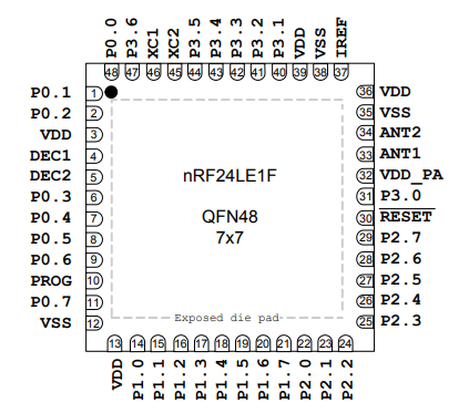
I went back over the datasheet some more and found that the flash programming SPI interface enabled by the PROG pin has its own set of assigned pins. These pins did not match up with the test pads I just wired up, so I checked to see if those were broken out on the remaining test pads. I used a multimeter continuity test to trace where these pins lead to, but you can also follow the traces in the picture of the nRF24 side of the PCB. Luckily the smaller test pads T10 through T13 do connect to these flash SPI interface pins (P1.2, P1.5, P1.6, and P2.0). Since there were only four more pads, I used my PCBite probes again instead of soldering more wires up.
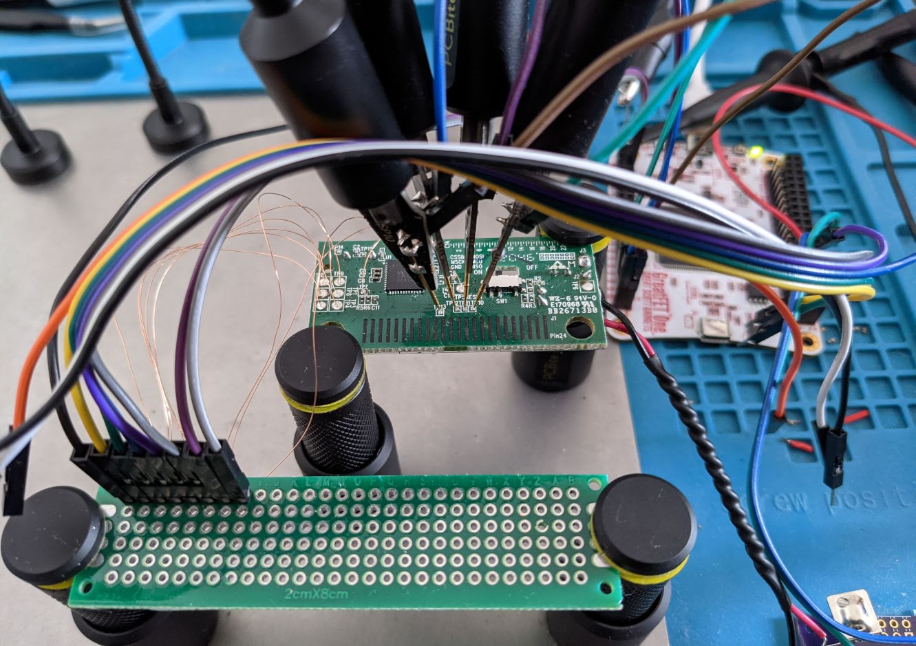
Enabling the flash programming SPI interface requires holding the PROG pin high and resetting the device by pulsing RESET low. I set up another GPIO pin on the GreatFET for the PROG pin, and then added a function to my test script for pulsing the RESET pin low.
#!/usr/bin/env python3
import hexdump
import time
from greatfet import GreatFET

def reset(gf, reset_pin):
    reset_pin.low()
    time.sleep(0.001)
    reset_pin.high()
    time.sleep(0.001)


def main():
    gf = GreatFET()
    reset_pin = gf.gpio.get_pin('J1_P4')
    prog_pin = gf.gpio.get_pin('J1_P6')

    # Reset is active low
    reset_pin.high()

    # Enter prog mode
    prog_pin.high()
    time.sleep(0.01)
    reset(gf, reset_pin)

    # ...

if __name__ == '__main__':
    main()
After resetting the device I’d attempt to send one of the flash SPI commands to get the flash status and flash protection status registers, as well as do a test read:
fsr = ord(gf.spi.transmit([0x05], receive_length=1))
fpcr = ord(gf.spi.transmit([0x89], receive_length=1))
print(f'flash status register: {fsr:#02x}')
print(f'flash protect register: {fpcr:#02x}')

# test read
print('test read:')
data = gf.spi.transmit([0x03, 0x00, 0x00], receive_length=256)
hexdump.hexdump(data)
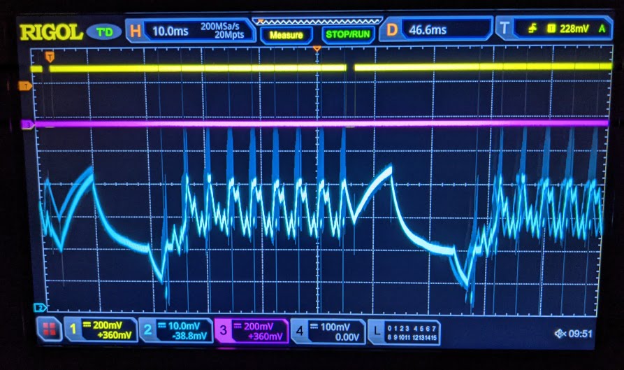
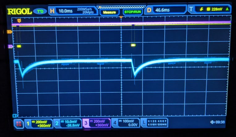
I still wasn’t getting any response (just the same series of 0xFF bytes), so I did a bit of debugging with my oscilloscope to make
sure all the pins were working correctly. I ran a simple script on the GreatFET to keep
resetting the device and triggered the oscilloscope on the reset pin going back up high
so I could look at the state of the scope probes soon after boot.
In addition to checking the RESET and PROG pins,
I took a simple power consumption measurement with a shunt resistor to see if the device
was really resetting. Note the difference in the power consumption when the device
successfully enters PROG mode:
One of the flash SPI probes might’ve been off, but after checking everything was OK on the oscilloscope I tried this process again and was able to read out some intelligible data from the flash:
$ ./test.py
flash status register: 0x80
flash protect register: 0x0
test read:
00000000: 80 A3 A3 02 00 03 78 FF  E4 F6 D8 FD 90 00 00 7F  ......x.........
00000010: 00 7E 04 E4 F0 A3 DF FC  DE FA 75 81 7E 02 07 82  .~........u.~...
00000020: FC 00 FF D9 00 11 01 FF  E0 FF E0 00 01 02 FF E1  ................
00000030: FF E1 00 01 02 FF E2 FF  E6 00 01 02 FF E7 FF EB  ................
00000040: 00 01 02 FF EC FF EF 00  04 02 FF F0 FF FF 00 01  ................
00000050: 00 57 69 72 65 6C 65 73  73 20 4B 65 79 62 6F 61  .Wireless Keyboa
00000060: 72 64 20 00 34 D9 1D F0  40 01 00 00 00 61 02 20  rd .4...@....a.
...
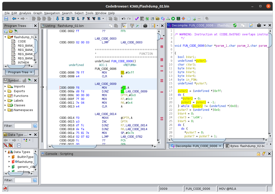
Note the “Wireless Keyboard” string. After that I did a single read for 18432 bytes, the maximum allowed according to the data sheet. The output looked liked a sensible dump of the program flash. The nRF24LE1 uses the 8051 instruction set, so to confirm it was code I loaded it into Ghidra as an 8051 binary blob. There appears to be an initialization routine near the beginning of the blob, suggesting it’s valid code.
To verify the flash readback protection and hardware debug enable settings I also wanted to read out the InfoPage mentioned in the datasheet:
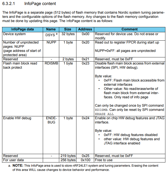
Reading the InfoPage requires setting the INFEN bit in the flash status register, so to do that I just had to send a “write flash status register” command before performing the read:
def read_fsr(gf):
    fsr = gf.spi.transmit([0x05], receive_length=1)
    return ord(fsr)

def write_fsr(gf, fsr):
    fsr &= 0xff
    gf.spi.transmit([0x01, fsr])

def read_flash(gf, address, count):
    command = struct.pack('>BH', 0x03, address)
    data = gf.spi.transmit(command, receive_length=count)
    return data

def get_infoblock(gf):
    flash_stat_reg = read_fsr(gf)

    # INFEN is bit 3 (2^3)
    write_fsr(gf, flash_stat_reg | 8)
    time.sleep(0.001)

    infoblock = read_flash(gf, 0, 512)

    # Unset INFEN bit
    write_fsr(gf, flash_stat_reg & (~8 & 0xff))

    return infoblock
Now I can read out the InfoPage to confirm the readback protection and HW debug settings. Although the fact that my initial read attempts returned program data also indicated that readback protection was disabled, going through these steps helped me build confidence that I was using the flash programming interface correctly. It looks like a backup of the InfoPage would also be important to have in case I erase the flash later on.
With a few more simple additions it’s easy to use this code to dump the program flash and/or InfoPage out to files:
$ ./k360_spi.py --dump flashdump.bin
flash status register: 0x80
flash protect register: 0x0
InfoBlock content:
00000000: 00 A3 A3 48 31 57 54 79  70 14 0A 12 FF FF 98 04  ...H1WTyp.......
00000010: 79 7C 88 23 B1 50 0F 05  FF FF FF FF 82 79 FF FF  y|.#.P.......y..
00000020: FF FF FF FF FF FF FF FF  FF FF FF FF FF FF FF FF  ................
00000030: FF FF FF 4C 45 31 4F FF  FF FF FF FF FF FF FF FF  ...LE1O.........
...
000001F0: FF FF FF FF FF FF FF FF  FF FF FF FF FF FF FF FF  ................
Flash readback protection: False (ff)
HW debug enabled: False (ff)
wrote flash dump to flashdump.bin
The full source code for k360_spi.py can be found at https://gist.github.com/jamchamb/b2892a22ac0760346d4d617fedf9b541. The next step will be to analyze the firmware.